Introduction
This article covers the process of ordering PCBs from JLCPCB, after finishing the schematic and board layout in KiCad.
JLCPCB is a company based in Shenzhen, China, offering PCB manufacturing and assembly (PCBA) services, making it possible for individuals to manufacture electronic boards cheaply and quickly. Several similar services exist, and I had used Elecrow before, but since it had been a while since my last PCB order, I decided to try the popular JLCPCB for the first time.
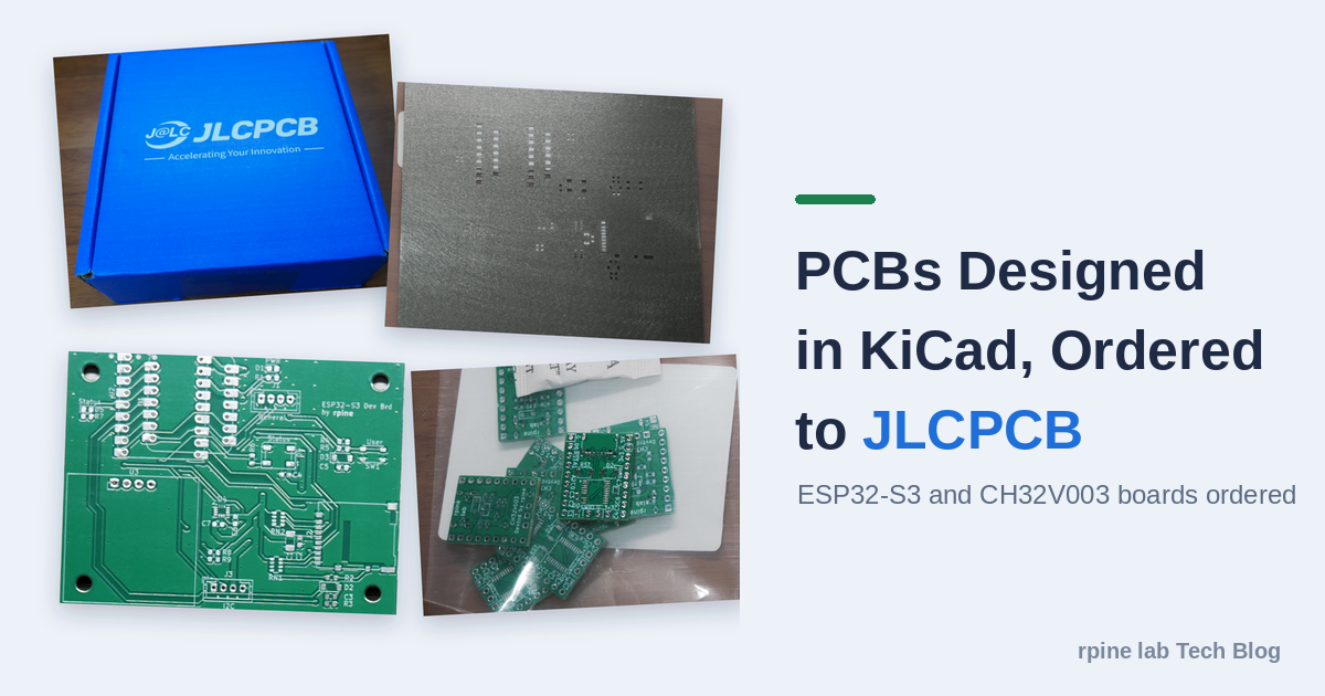
This time, I ordered two boards, an ESP32S3 carrier board and a CH32V003 prototype board, plus a solder reflow stencil.
.DwlzylGa.jpg)
ESP32S3 Carrier Board
A board that carries an SD card slot, an IMU, and an I2C display module, for experimenting with ESP32-S3-based microcontroller boards such as the XIAO ESP32-S3 and inexpensive Chinese ESP32-S3 boards.
CH32V003 Prototype Board
A general-purpose microcontroller board built around the CH32V003F4P6, a cheap chip (50 yen per chip at the time of purchase, 60 yen as of August 2026 by Akizuki Denshi).
A previous blog post using the same chip (in Japanese):
格安RISC-VマイコンCH32V003をMounRiver Studio Ⅱで開発してみる
Prerequisites and Environment
- Prerequisite: schematic and board layout already completed in KiCad
- Environment: Windows 11, KiCad 10.0.5
KiCad Settings
Skip the detailed KiCad design steps.
Design Rule Settings
From the board setup screen, I configured constraints that match JLCPCB's manufacturing capabilities (reference: PCB Manufacturing and Assembly Capabilities - JLCPCB). With this set, running DRC (design rule check) lets you confirm the design meets the manufacturing constraints.
Ideally you want some margin over the manufacturing limits, but not every requirement can be set here, so some compromises are necessary.

For the minimum clearance between traces, the manufacturing limit is 0.1 mm, but I set 0.15 mm for some margin. The clearance from conductors to holes differs between plated holes (PTH, 0.28 mm) and non-plated holes (NPTH, 0.2 mm), but since they can't be set separately, I matched it to the plated-hole value.
Microvias aren't used this time, so they can be ignored.
For the silkscreen, the minimum size in the manufacturing spec is a 1 mm text height and 0.15 mm stroke width, but you can go smaller if you accept the risk of it blurring out and becoming illegible in the worst case. This time I used a height of 0.8 mm in one spot only (see the result later).
Other fine-grained constraints can also be added. For example, adding the following rule as a KiCad custom rule lets DRC detect the clearance between pads and silkscreen.
(version 1)
(rule "Pad to Silkscreen"
	(layer outer)
	(condition "A.Type == 'Pad' && B.Layer == '?.Silkscreen'")
	(constraint silk_clearance (min 0.15mm))
)
Routing Settings
I used the following settings when routing the boards this time.
- Trace width
- Signal traces: 0.25 mm
- Power traces: 0.5–1 mm (thicker depending on the allowable current)
- Via settings
- Standard (for signal traces): 0.6 mm pad diameter, 0.3 mm hole diameter
- Power lines: larger as needed (e.g. 0.8/0.4 mm), or multiple vias in parallel
Setting up net classes like this is convenient during routing.

Preparing the Order Files
When placing an order, you need to generate the board's manufacturing files (Gerber files, drill files) and bundle them into a ZIP file.
You can build the ZIP file by hand, but it's quicker to use the community-made Fabrication Toolkit plugin, which generates the JLCPCB order data in one go.
Installing the Plugin
- From KiCad's project window (the initial screen), open the Plugin and Content Manager
- Search for Fabrication Toolkit and click install on the matching plugin
- Clicking Apply Pending Changes completes the plugin installation
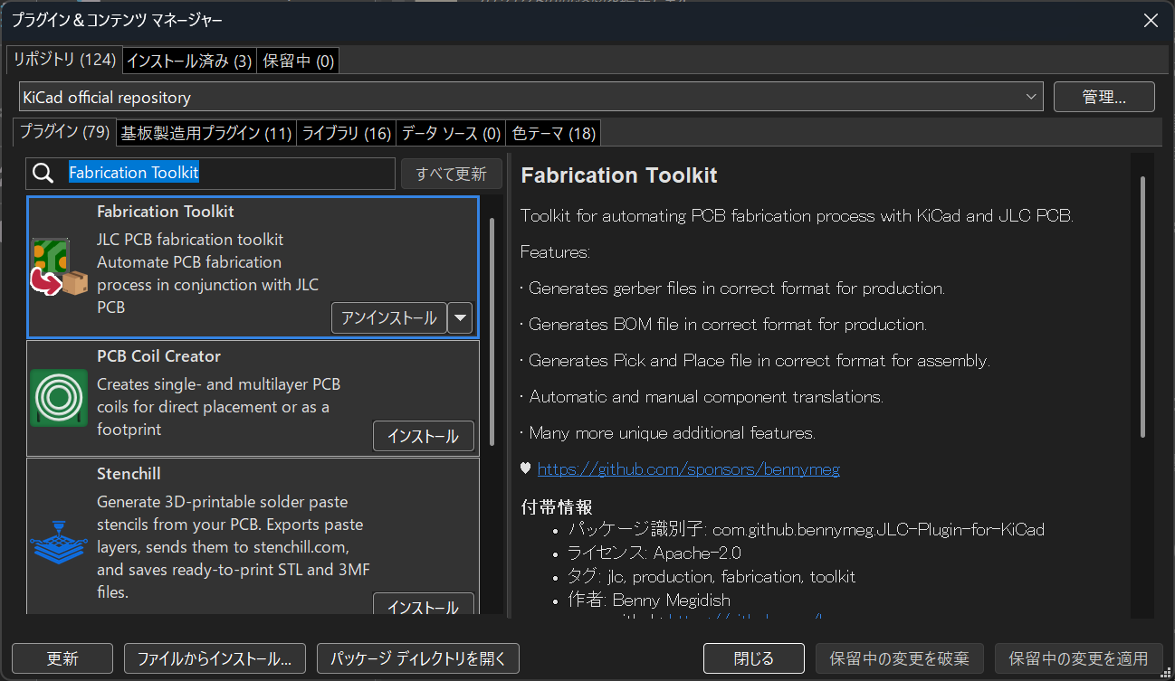 Plugin manager screen (after installation)

Generating the Order Files
- Click the Fabrication Toolkit icon in the PCB editor's top toolbar
- Leave the settings as they are and click Generate

The submission files are generated inside the KiCad project's production folder. The PCBA (assembly) BOM file isn't needed this time, so only the ZIP file is required.

Ordering on JLCPCB
The information below reflects the situation at the time of ordering (August 2026), so please check the actual quote page for details, especially pricing.
Using the JLCONE Desktop App
You can order directly from the JLCPCB website, but ordering through a desktop app called JLCONE seems to offer a discount, so this time I downloaded that app and placed my order through it.
After installing and launching it, a dedicated browser opens showing the JLCPCB site, and from there the process was the same as ordering through the site.
Uploading the Gerber Files
Uploading the generated ZIP file from the JLCONE app's quote screen shows a preview of the board and automatically fills in the dimensions.

Selecting Manufacturing Options
You select the board thickness, color, surface finish, and so on. The estimated price updates every time a setting changes.
I don't have particular preferences, so I left everything at the default except quantity.
- Layers: 2 (double-sided)
- Dimensions: kept as auto-filled
- Quantity: 5 ESP32S3 carrier boards, 10 CH32V003 prototype boards
- Board color: green (other colors add two extra manufacturing days)
- Board thickness: 1.6 mm
- Copper weight: 1 oz
- Surface finish: HASL with lead

Adding a Stencil
This time I also ordered a reflow stencil, for the ESP32S3 carrier board only. To order a stencil, turn on the stencil toggle near the bottom of the quote screen.
There are several settings, but I only changed the dimensions this time.
You can choose a standard or custom size. With custom size, entering your own dimensions gives a smaller stencil than the standard size. The standard size assumes mounting in the factory's automated paste-dispensing machine and is oversized for individual use, so a custom size works fine if you're applying solder paste by hand. In my testing, staying within 100×100 mm made it cheaper than the standard size. That said, making the stencil exactly the same size as the board makes it hard to hold in place, so it's better to leave a few extra centimeters on each side.

Shipping and Payment
Once you finish entering everything, add it to the cart and proceed to checkout, where you enter the shipping address and so on.
That's where you choose a shipping method. The quote (order) screen also shows the list of shipping methods, with estimated business days and cost varying by carrier. Among them, OCS Express is affordable and worth recommending. OCS is part of the ANA Group, so it seems reliable. There's also the cheaper OCS NEP, but it's limited to shipments under 0.6 kg, so it suits small orders.
You can pay with PayPal, Google Pay, or a credit card. Checking on the order screen, PayPal and Google Pay both carry payment fees, so I just paid by credit card. Since it's billed in US dollars, I paid with a Revolut card, which has favorable exchange rates.
The total came to $6.75 for the items (two board types plus one stencil) + $3.80 shipping = $10.55. The item total is quite low thanks to first-time coupons and similar discounts.
Responding to the Post-Order Confirmation Email
After placing the order, a JLCPCB engineer reviews the data. If it trips any of the factory's design rules (clearances and other constraints), you may receive a confirmation email.
This time I was asked a question by email about the stencil. It concerned how to handle a spot where a drill hole overlapped with a pad, and it arrived as an English email with an image of the manufacturing file attached.

The flagged spot was where the microcontroller board mounts: I had placed both a through-hole for the pin header and an edge-castellation pad for direct-mount soldering of the microcontroller board.

They offered three options as reference and asked which I'd like:
- A. Open the pad only, excluding the drill hole (direct-mount pad only)
- B. Open both the pad and the drill hole (both the direct-mount pad and the pin-header through-hole)
- C. Open neither the pad nor the hole (no paste at the mounting area, hand soldering only)
I ruled out option B, since solder paste would get into the pin-header through-hole. This spot was originally meant for hand soldering, so option C would have worked too, but I went with option A, opening a stencil hole on the pad only, so I could also try direct-mount soldering. If I don't end up needing paste there, I can just avoid that spot while applying it, or cover the hole with tape.
Checking the solder paste layer of the submitted Gerber data, the stencil wasn't open at that spot. It seems JLCPCB deliberately cross-checked it against the other board layers and reached out about it.
I replied briefly by email in English, saying to go with Option A.
The actual reply email
Hi
[sender name],Thank you for checking on this.
Please go with option A (open pads without drill holes).
Best Regards,
[my name]
Five minutes (!) after I replied, the person in charge got back to me and manufacturing resumed.
Manufacturing Progress
You can track the manufacturing progress at the factory in real time from "View Progress" at the top of the order details page.

It's impressive how far the production management goes, tracking things down to fine-grained manufacturing stages.
By the way, pressing the ▶️ button at each stage plays a reference video of the factory's production process, which is fun to watch.

Manufacturing started the day after ordering and finished in exactly two days.
Arrival and Inspection
It arrived exactly one week after ordering. I used OCS as the carrier, and within Japan it was handed off to Yamato Transport for home delivery. As shown in the photos, it arrived as a blue cardboard box inside a blue plastic bag.


Inside the box were the boards and the stencil, packed with cushioning material, and the boards were sealed in a bag with desiccant. The quantities matched the order: 5 ESP32S3 carrier boards, 10 CH32V003 prototype boards, and 1 stencil.


Looking at the actual boards, both the PCBs and the stencil came out clean. On the silkscreen, one spot (the "SWIO" label at the 5th pin from the top on the right, in the CH32V003 board photo) came in below the spec's minimum size at a height of 0.8 mm, but since the character shapes are simple, it printed without any real problem. I haven't checked for fine wiring shorts or continuity elsewhere, but everything looks fine at a glance.
Summary
This article covered the process of ordering PCBs I designed in KiCad from JLCPCB. The total cost was $10.55 (including first-time discounts) for two board types (5 + 10 boards) plus one stencil, and it took one week from order to arrival. It's cheap, fast, and easy, so I plan to keep using it going forward.
Next time, I'd like to try a configuration built mainly from parts in JLCPCB's stock, and give PCBA (assembly service) a try as well.
Details of the boards I designed are planned for separate articles (an ESP32S3 carrier board edition and a CH32V003 prototype board edition).
References
- KiCad (circuit design tool): https://www.kicad.org/
- Fabrication Toolkit (KiCad plugin): https://github.com/bennymeg/Fabrication-Toolkit
- JLCPCB (PCB ordering site): https://jlcpcb.com/
- JLCPCB manufacturing specifications: https://jlcpcb.com/capabilities/pcb-capabilities
- JLCONE Desktop (JLCPCB ordering desktop app): https://jlcpcb.com/download
- Revolut (virtual card with favorable exchange rates): https://www.revolut.com/
- OCS (the ANA Group carrier used for shipping): https://www.ocs.co.jp/