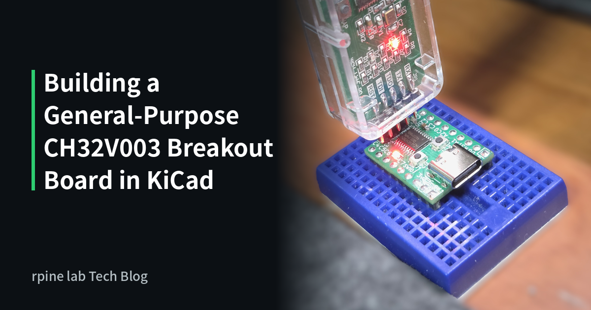
Overview
I made a general-purpose breakout board for the CH32V003, the low-cost microcontroller I have covered on this blog before.
I designed the board in KiCad and ordered it from JLCPCB, which has its manufacturing base in China.
I covered how I ordered the board in a separate article (Ordering Two Custom PCBs Designed in KiCad on JLCPCB). This article covers the board design, soldering the parts, and checking that it works.
Board specifications
- Microcontroller: CH32V003F4P6
- Form factor: two rows of 9-pin headers (rows 600 mil / 15.24 mm apart)
- All pins except those assigned to USB and the user LED are broken out
- Designed to match the size of a small, inexpensive ESP32-S3 board (ESP32-S3 Super Mini)
- Can be plugged into a perfboard or breadboard
- USB: for software USB with rv003usb, D+ (PD3), D− (PD4) and a circuit that controls the D− pull-up from PD5 are connected (details in the next article)
- Programming and debugging: a pin socket for the debugger (SWIO, GND, 3.3 V) on the board
- The WCH-Link plugs in directly for debugging
- MCU power: 3.3 V stepped down by a linear regulator from the 5 V on USB Type-C
- User LED: PD0 (lit when high)
- User button: PD2 (active low, external pull-up)
- Reset button: NRST (PD7)
Main parts
I bought the parts mainly from DigiKey and Akizuki Denshi.
- RISC-V microcontroller: CH32V003F4P6 (WCH)
- Where to buy: Akizuki Denshi, AliExpress 1 (bare chips), 2 (set with programmer, dev board and chips)
- 20 pins, TSSOP20 package
- Max operating frequency: 48 MHz
- Flash: 16 KB
- SRAM: 2 KB
- Small surface-mount tact switch (for reset and the user button): B3U-1000P (Aratas)
- Where to buy: DigiKey
- Size: 3.00 mm × 2.50 mm
- Picking a small tact switch ended up costing more per unit than the microcontroller. I plan to look for another switch of similar size.
- USB Type-C connector: UJ20-C-H-G-SMT-2A-P16-TR (Same Sky)
- Where to buy: DigiKey
- Linear (three-terminal) regulator: SL6206-33NR (Shenzhen Slkormicro Semicon Co., Ltd.)
- Where to buy: DigiKey
Board design
I designed the board in KiCad 10.
Schematic
The circuit is basically built from the recommended (application example) circuits in the datasheets of the parts used. On this board, the following parts follow the datasheets and specifications.
- Microcontroller
- Following the power supply example in the datasheet (Figure 3-1 Typical circuit for conventional power supply), a 0.1 µF decoupling capacitor sits close to the power pins (between VDD and VSS)
- Following the external reset example in the datasheet (Figure 3-5 Typical circuit of external reset pin), a 0.1 µF capacitor is added
- Linear regulator: 1 µF capacitors on the input and output
- USB circuit: follows the reference circuit in the rv003usb README (details in the next article)

Note: the regulator pinout in the schematic differs from the SL6206-33NR I actually used (see below).
Board layout


So that the board fits a breadboard, I set the spacing between the pin header rows to 15.24 mm (600 mil), a multiple of the 2.54 mm pitch, and decide the board outline from that. Once the outline is fixed, the rest is squeezing in the parts and traces.
Because of the size, not all parts fit on the front, so the regulator, the resistors around USB and some other parts are on the back.
The design rules mostly follow JLCPCB's manufacturing capabilities (reference). Power traces are 0.75 mm wide and other signal traces 0.25 mm. For the KiCad settings, see also the previous article (Ordering Two Custom PCBs Designed in KiCad on JLCPCB).
You can also create a silkscreen logo by loading a PNG logo file into KiCad's Image Converter.

Once most of the parts are placed, you can check a 3D model of the board from View → 3D Viewer (Alt + 3).

Assembly
Tools

- Soldering iron: FNIRSI HS-02A
- A USB PD-powered soldering iron. The temperature can be set finely, and it sleeps when not in use and wakes up as soon as you pick it up, which is handy.
- Solder wire: leaded solder in two diameters, 0.65 mm and 0.3 mm
- I prepared two diameters, but the 0.65 mm solder alone was enough this time.
- Desoldering braid
- When hand-soldering surface-mount parts, I use it to remove excess solder where a desoldering pump is hard to use.
- PCB flux
- If the solder stays molten for a long time, the flux in the solder wire burns off. When the solder does not form properly or the surface turns dull, I add more flux.
- Heat-resistant silicone mat for electronics work / craft mat
- Laid down so the desk does not get burned.
Soldering order

I mount the microcontroller (TSSOP20 package) first, then the USB Type-C connector, the remaining parts on the front, and finally the parts on the back (such as the linear regulator).
Soldering the TSSOP20

First I put solder on one pad and solder just one microcontroller pin to hold it in place. Then I touch the iron tip, loaded with solder, to the side of the pins and drag it along to solder the remaining pins.
If pins get bridged:
- Pull the excess solder onto the iron tip, or wick it up with desoldering braid
- Apply flux and touch the iron tip again, and the solder will reshape properly
Soldering the USB Type-C connector

Holding the connector down with reverse-action tweezers, I solder it the same way as the microcontroller, dragging the solder-loaded iron tip along the terminals. Because the pitch is narrow, I deliberately use plenty of solder, expecting bridges, and remove the excess afterwards with desoldering braid.
With the narrow pitch, and pins that barely stick out unlike the microcontroller's, this was the hardest part to hand-solder on this board.
Soldering the other surface-mount parts
This board mainly uses 1608 (1.6 mm × 0.8 mm, 0603 imperial) chip resistors and capacitors. At this size they were no problem to hand-solder.
Soldering chip resistors and capacitors:
- Put solder on one pad
- Hold the part with tweezers and tack one side while melting the solder on the pad
- If the part lifts, press it down while melting the solder so it sits flat on the board
- Flow solder onto the other side
- Remelt the first side to finish the joint

Checks before powering up
Using the continuity mode of a multimeter, I check that the power pins and ground are not connected, and that adjacent pins on the microcontroller and other parts are not shorted together (possible solder bridges).
Power-up test

I power the board and check that the parts other than the microcontroller work. As the power supply I use a portable constant-voltage/constant-current variable supply that runs from a USB PD charger (Alientek DP100), with the current limit set to 100 mA to keep the current low if there is a short.
First I feed 3.3 V directly to the 3.3 V pin and check the supply's current reading for overcurrent or shorts.
Next I apply 5 V and measure the linear regulator's output with a multimeter. Instead of the expected 3.3 V, it read somewhere in the 4 V range.
Linear regulator pinout mistake
Checking the datasheet of the regulator I bought, I found that its pin assignment differed from the KiCad schematic symbol.
When you use a generic schematic symbol, you need to check its pin assignment against the datasheet, and I had forgotten to do that.


Pins 1 and 3 were swapped, so I bent the pins the other way, flipped the regulator over and mounted it at a 45-degree angle, which got it working (please don't copy this). The "Assembled back side" photo above shows how it is mounted.
After remounting it, I measured again and confirmed a 3.3 V output. The microcontroller is also rated to run at 5 V, so it was not damaged.

For the second and later boards, I plan to use a separate linear regulator with the same pinout as the schematic (I have already secured the AP7375 from Akizuki Denshi).

Testing
Development environment
I use MounRiver Studio Ⅱ, the IDE I covered in an earlier article, as the development environment.
For setup and other details, see the following article: Developing on the Low-Cost RISC-V Microcontroller CH32V003 with MounRiver Studio Ⅱ
This board has a 3-pin socket that the official WCH-Link debugger plugs into directly.
The socket has SWIO (debug signal), GND and 3.3 V (MCU power) in that order. This matches the order on part of the WCH-Link connector, so as the photo shows, you can plug it in directly to program and debug.

Test program
I modify the sample program (the template generated when creating a project) into a simple test program for LED blinking and button input.
static uint8_t cnt = 0;

void UserPins_Init (void) {
    GPIO_InitTypeDef GPIO_InitStructure = {0};

    RCC_APB2PeriphClockCmd (RCC_APB2Periph_GPIOD, ENABLE);

    GPIO_InitStructure.GPIO_Pin = GPIO_Pin_0;
    GPIO_InitStructure.GPIO_Speed = GPIO_Speed_50MHz;
    GPIO_InitStructure.GPIO_Mode = GPIO_Mode_Out_PP;
    GPIO_Init (GPIOD, &GPIO_InitStructure);  // UserLED
    GPIO_InitStructure.GPIO_Pin = GPIO_Pin_2;
    GPIO_InitStructure.GPIO_Mode = GPIO_Mode_IN_FLOATING;
    GPIO_Init (GPIOD, &GPIO_InitStructure);  // UserBtn
}

int main (void) {
    NVIC_PriorityGroupConfig (NVIC_PriorityGroup_1);
    SystemCoreClockUpdate();
    Delay_Init();
#if (SDI_PRINT == SDI_PR_OPEN)
    SDI_Printf_Enable();
#else
    // USART_Printf_Init (115200);
#endif

    UserPins_Init();
    GPIO_SetBits (GPIOD, GPIO_Pin_0);

    printf ("SystemClk:%d\r\n", SystemCoreClock);
    printf ("ChipID:%08x\r\n", DBGMCU_GetCHIPID());

    while (1) {
        uint8_t btnState = GPIO_ReadInputDataBit(GPIOD, GPIO_Pin_2);
        printf("Cnt:%03d", cnt);
        printf(" Btn:%d", btnState);

        // if (cnt & 0x1) { // LED blink test
        if (!btnState) { // Button input test
            GPIO_SetBits (GPIOD, GPIO_Pin_0);
            printf(" LED:On\n");
        } else {
            GPIO_ResetBits (GPIOD, GPIO_Pin_0);
            printf(" LED:Off\n");
        }

        cnt++;
        Delay_Ms(200);
    }
}
LED blink
The board has an LED connected to the microcontroller's PD0 pin, so I light it using GPIO.
The code above is for the button input test. To try the LED blink, uncomment the if (cnt & 0x1) line and comment out the if (!btnState) line. cnt increases by 1 about every 200 ms, so the LED blinks with a period of about 0.4 seconds.

Button input
I read the user button on the board through GPIO and check whether it is pressed.
Using SDI printf (which sends printf output to the WCH-Link over SWIO), I check the button state in the debug output.
Cnt:011 Btn:1 LED:Off
Cnt:012 Btn:1 LED:Off
Cnt:013 Btn:1 LED:Off
Cnt:014 Btn:1 LED:Off
Cnt:015 Btn:0 LED:On // On only while pressed
Cnt:016 Btn:0 LED:On
Cnt:017 Btn:0 LED:On
Cnt:018 Btn:0 LED:On
Cnt:019 Btn:1 LED:Off
Cnt:020 Btn:1 LED:Off
Cnt:021 Btn:1 LED:Off
Cnt:022 Btn:1 LED:Off
Cnt:023 Btn:1 LED:Off
Summary
I designed a general-purpose CH32V003 breakout board in KiCad, had it made by JLCPCB, hand-soldered it and confirmed that it works.
The power-up test turned up a pinout mistake on the linear regulator, but I got it working by mounting the part in a different orientation.
Next time, I will use the USB circuit on this board and rv003usb to connect to a PC over software USB.
References
- CH32V003 series
- CH32V003 datasheet: pin assignments, operating voltage and so on
- CH32V003 reference manual
- SL6206-33NR (DigiKey): datasheet for the linear regulator
- rv003usb (GitHub): software USB library and reference circuit
- KiCad
- MounRiver Studio